Building a TinyUSBboard rev3 PCB
To make this build process of the tinyUSBboard revision 3 (on veroboard) a little less laborious it is possible to create a single sided PCB where, once finished, the components can be applied to. This makes the build process faster and cleaner and maybe less error prone to novice builders.
It is possible to find many tutorials about etching PCB's at home and this article won't cover this process (Search for "diy etching pcb board" with Google).
The board Eagle files to etch the PCB can be found on BauweBijl's GitHub where you also can find some tips about printing. For the board in the example below the toner transfer method is used (which can be done with a laserprinter).
The PCB board is designed to use common available components as-well as the specified (and recommended) components from the tinyUSBboard-rev3 kit.
It uses a DIP socket as extra component to enable easy changes of various Atmega chips and there is enough space to use common 7.5 mm sized resistors (the tinyUSBboard revision 3 kit comes with smaller resistors).
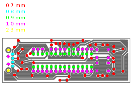
Drilling
Once finished a successful PCB etch the holes need to be drilled.
It depends on your drilling skills and available tools if this doable, there are many holes and it takes an amount of time.
The following drill sizes are needed to complete drilling the holes on the board.
- .7 mm
- .8 mm
- .9 mm
- 1.0 mm
- 2.3 mm
Drilling legend
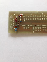
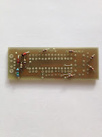
Solder the components in the following order
| Start the with resistors | Cut the component wires | Use the cuttings for the jumpers (4x) | ||
|---|---|---|---|---|
 |
 |
 |
| Solder the jumpers (*) | Solder the rest of the resistors | Place the socket (**) | ||
|---|---|---|---|---|
 |
 |
 |
(*) some jumpers will be hidden under the DIP socket later and cannot be accessed
(**) solder some pins ... not all ... the rest can be done later while soldering the headers
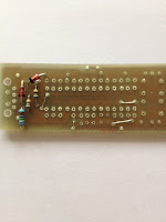
| Fold the USB clamps (*) | Solder the USB pins and clamps | Solder the push buttons | ||
|---|---|---|---|---|
 |
 |
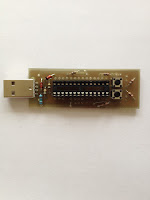 |
(*) fold these to the center and not to the side!
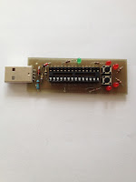
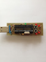
| The LED's | Solder the headers (*) | Solder remaining socket pins | ||
|---|---|---|---|---|
 |
 |
 |
(*) it's now a good time to solder the remaining pins from the socket (you only heat up the pad's once)
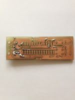
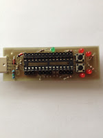
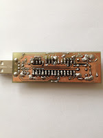
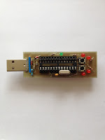
| Crystal and caps (*) and the fifth (**) jumper | Check traces carefully | Done! (***) | ||
|---|---|---|---|---|
 |
 |
 |
(*) the original tinyUSBboard rev 3 kit comes with the recommended 1uF capacitor (105) which skips one mounting hole ... a regular 0.10 uF capacitor (104) uses less space ... the board design allows placement of both types
(**) place the last jumper near the USB pins ... avoid contact with the wires by using wire insulation
(***) always test the board carefully before usage
Other infomation
TinyUSBboard rev3 PCB Eagle files on github
Labels: TinyUSBboard